
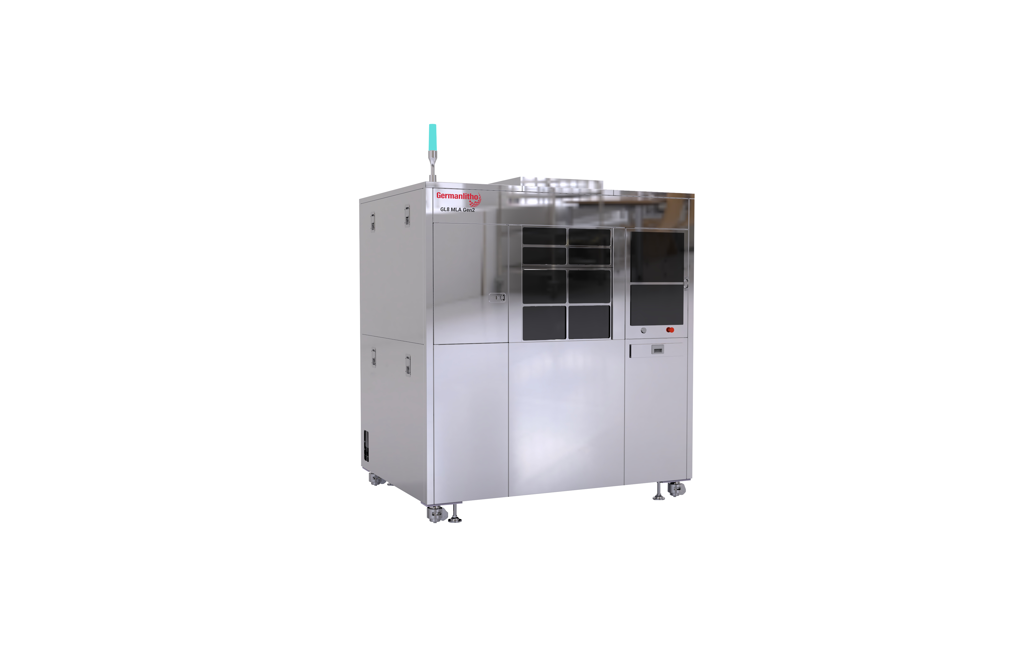
The GL8 MLA Gen2 is the GermanLitho latest semi-automatic UV nanoimprint lithography equipment developed dedicated for Wafer Level Optics (WLO) processes, which is capable of parallel imprinting polymer micro- and nano-optic components on up to 200 mm wafers.
GL8 MLA Gen2 supports automatic replication of flexible composite working stamps, which have the characteristics of high resolution and long service life, from wafer level master molds. Using working stamps can significantly reduce the cost of large-area molds in nanoimprint processes. The integrated high-precision automatic resist dispensing system, APC (Active mold/substrate Parallel Control) technology, and automatic separation function ensure fidelity, uniformity (TTV), and yield for large-area wafer level optics production. The automatic alignment system enables Wafer Level Stacking (WLS) processes. GL300 MLA is suitable for development and pilot production of DOE, Diffuser, MLA, Fresnel lenses and other products.
Volume-proven UV-nanoimprint equipment for Wafer Level Optics processes.
APC (Active mold/substrate Parallel Control) technology ensures large-area TTV uniformity of imprinted wafers.
Automatic replication of flexible composite working stamp, reducing the cost of large-area molds in nanoimprint processes.
Including automatic high-precision resist dispensing function.
Fully automatic process including working stamp replication, alignment, imprinting, curing and separation, etc.
High power UV LED panel light source (365nm, light intensity >1000mW/cm2) with water cooling, possible customization of power and wavelength of the light source, perfectly support a variety of commercial nanoimprint materials.
Mini-environment and electrostatic elimination device are equipped as standard.
A set of WLO nanoimprint processes and materials starter-kit will be delivered together with the machine, to enable our customers beginning with world leading level of nanoimprint technology based on our experiences.
Substrate size |
2inch, 100mm, 150mm, 200mm (Special sizes can be customized) |
Substrate material |
Silicon, glass, quartz, plastic, metal, etc. |
Wafer loading & unloading |
Single wafer automatic loading and unloading |
Wafer pre-alignment |
Optical pre-alignment |
Supported NIL process |
UV-NIL with APC (Active mold/substrate Parallel Control) technology, suitable for large area WLO, WLS and other processes |
Resolution |
Better than 10 nm* |
Aspect ratio |
Better than 10: 1* |
TTV control |
Micrometer accuracy (200mm wafer) * |
UV curing light source |
High power UV LED panel light source (365nm), light intensity >1000mw/cm2 (2000mw/cm2 optional) |
Mini-environment and climate control |
Standard, external environment class 100, internal environment better than class10* |
Automatic imprinting |
Supported |
Automatic separation |
Supported |
Automatic resist dispensing |
Supported |
Automatic working stamp replication |
Supported |
Automatic alignment |
Optional |