
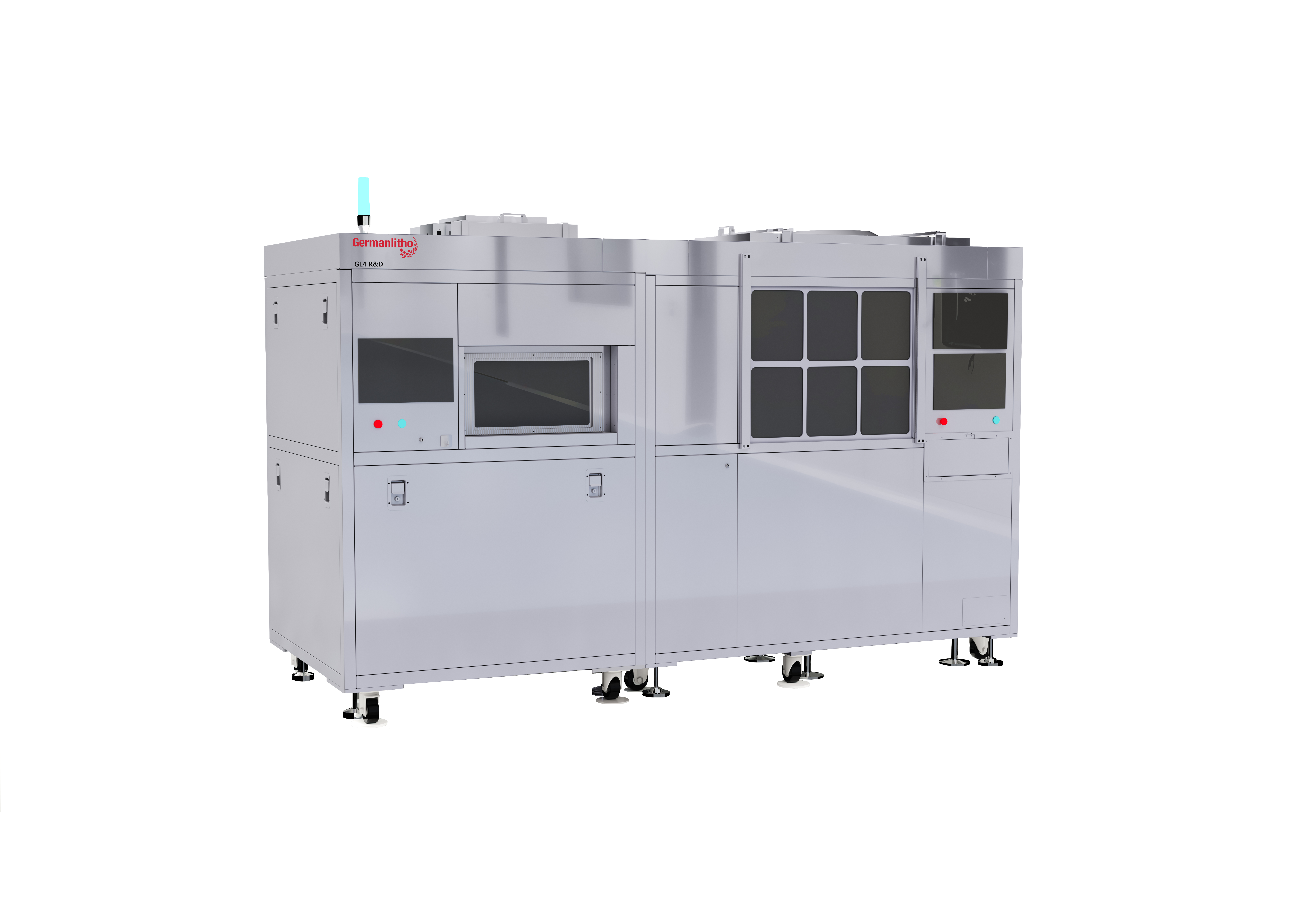
GL4 R&D is a powerful multi-functional nanoimprint lithography (NIL) equipment designed specifically for universities, research institutes and enterprise R&D departments.
The equipment can be configured with multiple nanoimprint modules: high resolution UV-NIL module, WLO (Wafer Level Optics) NIL module, and thermal NIL (HE - Hot Embossing) module. Versatile NIL processes can be carried out in one flexible machine.
The UV-NIL module enables imprinting of high resolution (better than 10nm *) and high aspect ratio (better than 10:1 *) nanostructures on up to 100mm spin-coated wafers. The WLO NIL module equipped with precise resist dispensing system and APC (Automatic mold/substrate Parallel Control) technology, ensures the imprint fidelity, large-area uniformity and yield for wafer level optics imprinting. The alignment system enables Wafer Level Stacking (WLS) process. The use of uniform gas pressure in thermal NIL module ensures large-area imprinting uniformity and replication fidelity.
GL4 R&D is suitable for the development of a wide range of nanoimprint processes, rapid device prototyping, nanoimprint material testing and other R&D activities. Following the process and material system of GermanLitho mass production nanoimprint equipment, the developed processes can be adapted to the mass production equipment straightforward. Application fields of GL4 R&D include DOE, AR waveguide (including slanted grating), WGP, metalens, biochip, LED, MLA, diffuser etc.
Following the process and material system of GermanLitho mass production nanoimprint equipment, the developed processes can be adapted to the mass production equipment straightforward.
Flexible optional configurations including high resolution UV-NIL module, WLO NIL module and thermal NIL module. Quick and easy switching between modules.
Max. imprinting area Φ100mm.
Automatic replication of flexible composite working stamp in the equipment, reducing the cost of large-area molds in nanoimprint processes.
Automatic NIL process including working stamp replication, imprinting, curing and separation, etc.
APC (Active mold/substrate Parallel Control) technology used in the WLO module ensures large area TTV uniformity of imprinted wafers. Including automatic high-precision resist dispensing function.
Uniform gas pressure up to 50bar (80bar can be customized) ensures large-area imprinting uniformity and replication fidelity in thermal NIL processes. UV and thermal-NIL processes can be carried out separately or in-situ in one imprint sequence simultaneously in thermal NIL module.
High power UV LED panel light source (365nm, light intensity >300mW/cm2), possible customization of power and wavelength of the light source, perfectly support a variety of commercial nanoimprint materials.
Optional alignment function.
A set of nanoimprint process and material starter-kit will be delivered together with the machine, to enable our customers beginning with world leading level of nanoimprint technology based on our experiences.
Configuration option |
UV-NIL module |
WLO imprint module (optional) |
Thermal NIL module (optional) |
Substrate size |
20x20mm substrate, 2inch, 3inch, 100mm wafers(Special sizes can be customized) |
||
Substrate material |
Silicon, glass, quartz, plastic, metal, etc. |
||
Supported NIL process |
High resolution UV-NIL on spin-coated wafers UV-NIL for WLO process(optional) thermal-NIL (Hot Embossing - HE) process (optional) Simultaneous UV-NIL & thermal-NIL in one imprint sequence (optional) |
||
Resolution |
Better than 10 nm* |
||
Aspect ratio |
Better than 10:1* |
||
|
Residual Layer Thickness(RLT) /TTV control |
RTL less than 10nm* |
TTV in μm accuracy* |
RTL less than 10nm* |
UV curing light source |
High power UV LED panel light source (365nm), light intensity >300mw/cm2 |
||
Automatic imprinting |
Supported |
||
Automatic separation |
Supported |
||
Automatic working stamp replication |
Supported |
||
Automatic resist dispensing |
/ |
Supported |
/ |
APC (Active mold/substrate Parallel Control) |
/ |
Supported |
/ |
Pressure application method |
/ |
/ |
Uniform gas pressure guarantees large-area imprint uniformity |
Imprint pressure |
/ |
/ |
≤50bar (80bar customized) |
Imprint Temperature |
/ |
/ |
RT ~ 250℃, setting accuracy ±1℃ |
Mini-environment and climate control |
Standard, external environment class 100, internal environment better than class10* |
||
Alignment |
Manual alignment, automatic alignment (optional) |
||
Wafer loading & unloading |
Manual loading and unloading |
||