
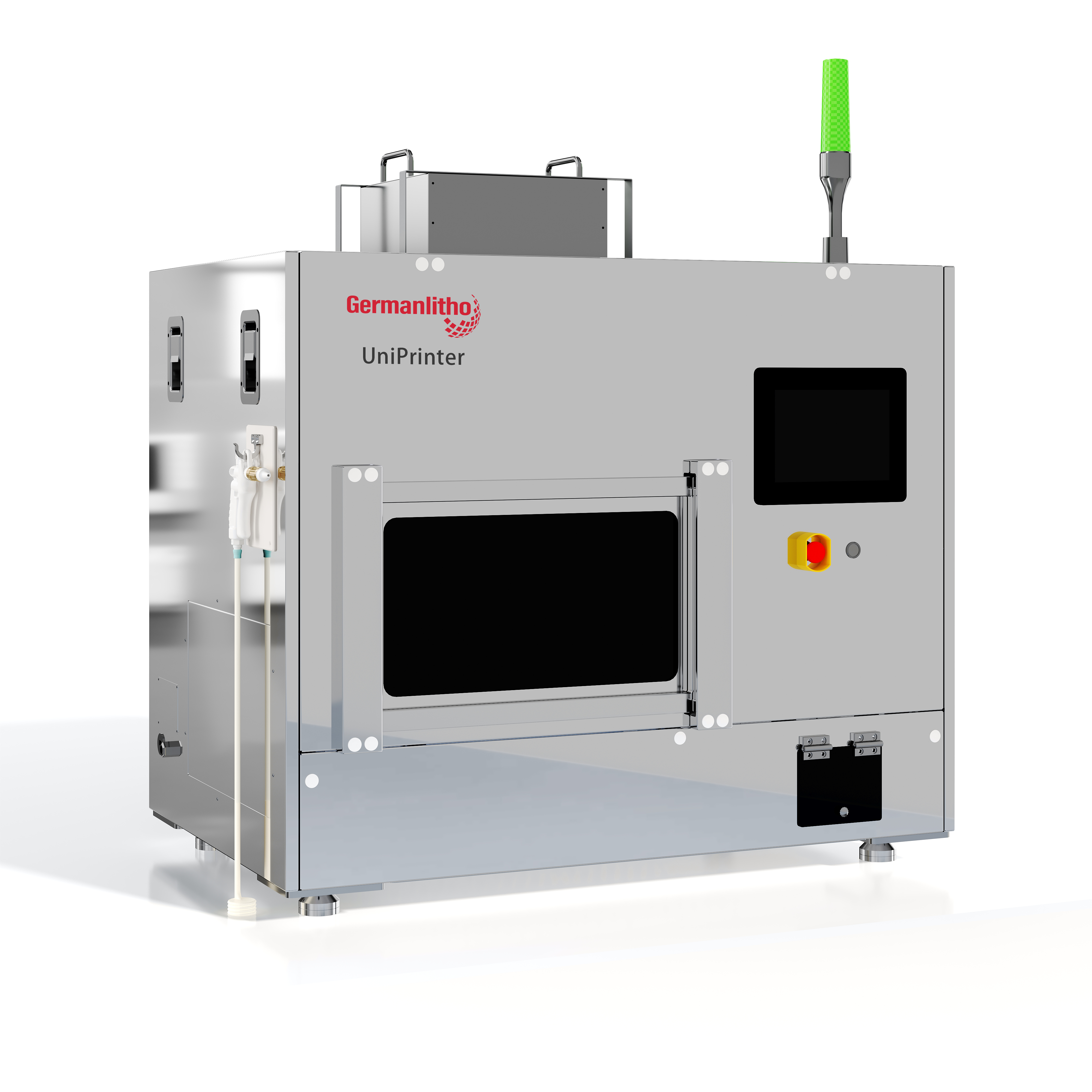
UniPrinter is a simple-operation and powerful desktop nanoimprint lithography (NIL) equipment designed specifically for universities, research institutes and enterprise R&D activities.
It enables imprinting of high resolution (better than 10nm*) and high aspect ratio (better than 10 : 1*) nanostructures on up to 4 inch wafers. UniPrinter is suitable for the development of UV nanoimprint lithography process, rapid device prototyping, nanoimprint material testing, etc.. It follows the process and material system of GermanLitho mass production NIL equipment. The processes developed on UniPrinter can be adapted to GermanLitho mass production equipment straightforward. UniPrinter is suitable for R&D of DOE, AR waveguide (including slanted grating), WGP, metalens, biochip, LED PSS and other applications.
Following the processes and material system of GermanLitho mass production nanoimprint equipment, the developed process can be adapted to the mass production equipment straightforward.
Imprinting of high resolution, high aspect ratio nanostructures on up to 100mm wafers.
Automatic replication of flexible composite working stamps in the equipment.
Fully automatic process including working stamp replication, imprinting, curing and separation, etc..
High power UV LED panel light source (365nm, light intensity >300mW/cm2), perfectly support for a variety of nanoimprint materials.
A set of nanoimprint process and material starter-kit will be delivered together with the machine, covering processes for DOE, AR slanted grating, high density, high aspect ratio structures etc., to enable our customers beginning with world leading level of nanoimprint technology based on our experiences.
Substrate size |
Up to 100mm wafers (special size can be customized) |
Substrate material |
Silicon, glass, quartz, plastic, metal, etc. |
Supported NIL process |
UV-NIL process, suitable for imprinting of high resolution, high aspect ratio nanostructures |
Resolution |
Better than 10 nm* |
Aspect ratio |
Better than 10:1* |
Residual layer thickness(RLT) |
Less than 10nm* |
UV curing light source |
High power UV LED panel light source (365nm), light intensity >300mW/cm2 |
Automatic imprinting |
Supported |
Automatic separation |
Supported |
Automatic working stamp replication |
Supported |
Wafer loading & unloading |
Manual loading/unloading |